
Giving every footprint a 3D model: EasyEDA, Python and a visual check
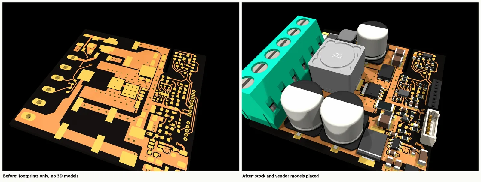
A circuit board can be correct on paper and still not fit in its box. A connector might face the wrong way, or a tall capacitor might hit the lid. A 3D view of the assembled board catches these problems before you order it. But the 3D view is only as good as the models behind it.
This article describes how we gave every part on a small power board a 3D model in KiCad. We used ready-made library models where they fit, and downloaded exact manufacturer models from EasyEDA for the rest. The interesting part was checking that each model sits correctly. For that, we rendered the board, cut out every part into a grid of close-ups, and looked at them, one tile at a time.
The board had been designed in an older tool and imported into KiCad. The import kept the copper pads, but most parts arrived without any 3D model. Others had models that were hidden or pointed the wrong way. An AI coding assistant wrote most of the Python scripts and read the image grids alongside us. The method works just as well by hand.
A few terms
- Footprint: the copper pads a part is soldered to, plus its outline. This is what gets manufactured.
- 3D model: a STEP or VRML file of the part's body. It is attached to a footprint and only affects the 3D view and exported models.
- LCSC number: the catalogue number of a part at LCSC, the distributor used by the JLCPCB assembly service, for example C2915640.
- Stock library: the footprints and 3D models that ship with KiCad.
Step 1: Take inventory and sort the parts
Start with a list, not with the 3D viewer. A KiCad board file (.kicad_pcb) is plain text, so a short Python script can walk through every footprint. For each one it records the reference (R5, D2, X1), the footprint name, the attached model if any, and the part's LCSC number from its properties.
That list splits the parts into three groups:
| Group | Typical parts | What to do |
|---|---|---|
| Standard packages | 0402–1206 resistors and capacitors, SOT-23, SOD-323, SMB/SMC diodes | Use KiCad's stock model, or swap to the stock footprint, which already has one |
| Specific parts | Terminal blocks, connectors, power inductors, ICs with an exposed pad | Download the manufacturer's exact model from EasyEDA by LCSC number |
| Parts with no data anywhere | Rare inductors, discontinued parts | Use a close stock model or the maker's own STEP file, or leave it and note it |
For the passives we went one step further and swapped the imported footprints for KiCad's stock ones. The stock pads were smaller and sat inside the old pad areas, so every track still ended on copper. The swap brought the stock 3D models along for free.
For the other parts we kept the imported copper exactly as it was and only attached a model. This is the safe choice when a board has already been checked or built: the copper doesn't change, so nothing can break electrically.
To decide whether a stock model fits, compare pad sets, not names. The script printed both footprints' pads side by side: number, position and size. The output showed whether the package was really the same and whether it needed rotating. For example, the imported 0603 LED had its pads stacked vertically with the cathode at the top. KiCad's stock LED lies horizontally, so it needed a 90° turn.
Step 2: Download exact models with easyeda2kicad
EasyEDA, the online design tool tied to LCSC and JLCPCB, holds a footprint and a 3D model for a large share of LCSC's catalogue. The open-source Python tool easyeda2kicad fetches them by LCSC number and converts them to KiCad formats.
We installed it in a throwaway virtual environment, so nothing touched the system Python:
python -m venv venvvenv/Scripts/pip install easyeda2kicad
Then one command per part downloads the footprint and the model:
for id in C413462 C146440 C151266 C2915640; do venv/Scripts/easyeda2kicad --lcsc_id $id --footprint --3d --output dl/lcsc --overwritedone
Each run adds a .kicad_mod footprint to dl/lcsc.pretty and a .wrl and .step model to dl/lcsc.3dshapes. Fetch the footprint even if you only want the model. The model was drawn to fit EasyEDA's footprint, so that footprint is your reference for placing the model on your own pads.
Nine of our eleven parts downloaded cleanly. For the other two, EasyEDA had no data. We searched LCSC for other listings of the same package and found none with a model. One part got KiCad's stock model for its standard package. The other, an unmounted option part, was left without a model and noted.
The downloaded .step files go into a folder inside the project, and footprints point at them through KiCad's project path variable: ${KIPRJMOD}/project.3dshapes/part.step. That keeps the project self-contained when you copy or share it.
Two practical notes:
- easyeda2kicad uses EasyEDA's unofficial web API. A day after our run, the same API started returning "403 Forbidden". Download what you need in one go and keep the files in the project.
- Comparing the vendor footprint with yours is a free design review. Ours showed that the terminal block's holes were 1.397 mm while the manufacturer's footprint used 1.5 mm. We widened them.
Step 3: Place each model on its pads
In the board file, a model is a short block inside its footprint. It names the file and gives an offset in millimetres, a scale and a rotation in degrees:
(model "${KIPRJMOD}/project.3dshapes/LED0603-RD_GREEN.step" (offset (xyz 0 0 0)) (scale (xyz 1 1 1)) (rotate (xyz 0 0 90)))
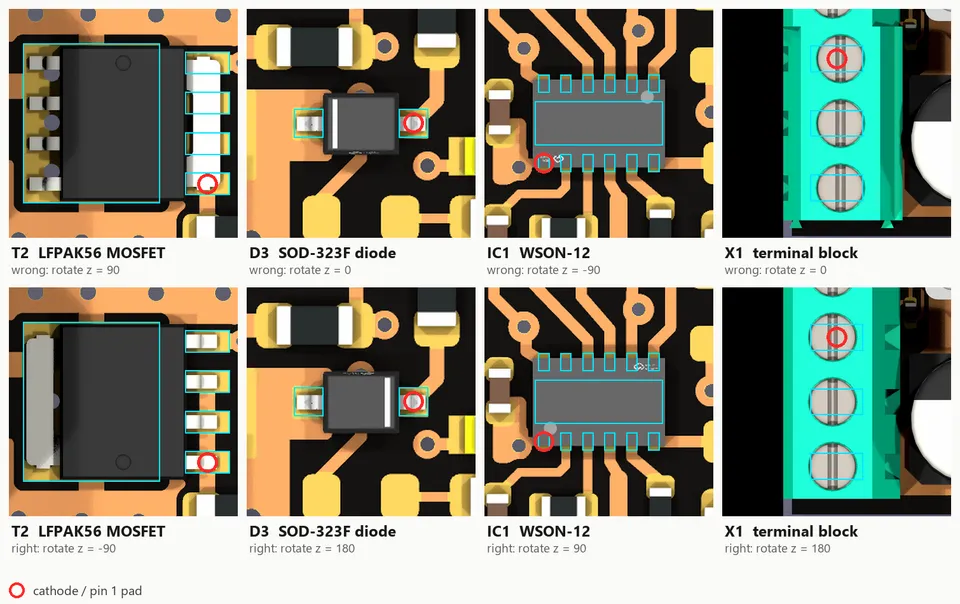
For most parts, getting it right comes down to one number: the rotation around the vertical axis. Work it out by comparing your pads with the vendor footprint the model was built for. If the vendor footprint has pin 1 on the left and yours has it at the top, the model needs a quarter turn.
The rotation sign is a trap. The value KiCad wants in the file is the mirror image of what ordinary geometry gives you. In our first attempt a MOSFET we had worked out as +90° rendered 180° off; it needed −90°. After that we never trusted a computed angle. We wrote the script, rendered the board and looked at the result.
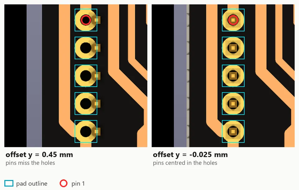
Offsets usually stay at zero. Most vendor models are centred on their footprint. Connectors are the exception. Our 5-pin wire-to-board header sat about 0.48 mm off its holes, which only shows up when you look at the board from below. To fix it, a script read every point in the STEP file below the board surface (the pin ends), grouped them into pins and compared their centres with the pad positions. One more trap: KiCad applies the model offset with the Y axis pointing up, while the board's Y axis points down. The pins only lined up after we flipped the sign of the measured Y offset.
Check that the model is actually visible. Footprints imported from other tools often have no type (neither SMD nor through-hole). KiCad treats such footprints as "virtual" and hides their models in the 3D view by default. Several of our models were already correct but invisible. Setting the footprint type fixed them all.
All of these edits were made by one Python script that rewrites the board file and the project's footprint library. Three habits kept it safe:
1. Close KiCad first, or at least check that its lock files (~*.lck) are gone. A save from the open editor will silently overwrite a script's changes.
2. Run the script on a scratch copy of the project. Render it and run the design rule check (kicad-cli pcb drc --schematic-parity). The number of warnings should not change.
3. Back up the board and footprints, then run the same script on the real project.
Step 4: Check every part by eye, in one image
A model can sit perfectly on its pads and still be wrong: a diode turned 180° looks fine until you notice the band is on the anode. Turning the board around in the 3D viewer to check twelve parts is slow, and easy to get wrong. Instead, we made one image that shows every part at once.
The recipe has three steps.
1. Render the board straight from above. KiCad's command-line tool renders without opening the GUI. An orthographic (non-perspective) top view keeps millimetres proportional to pixels everywhere on the board:
kicad-cli pcb render --side top --zoom 1 -w 2400 -h 2400 --quality high -o top.png board.kicad_pcb
2. Work out how board millimetres map to image pixels. The board is centred in the image, so you need only one number: pixels per millimetre. Measure it, don't guess it. Our script finds the top and bottom board edges in the render and divides their distance in pixels by the board height in millimetres from the board file. It also checks the result against a third edge.
def to_px(x_mm, y_mm): return (W / 2 + (x_mm - board_cx) * px_per_mm, H / 2 + (y_mm - board_cy) * px_per_mm)
3. Cut out each part and draw what it should look like. For every part the script crops a square around the footprint's centre and scales it to the same tile size. On top of each tile it draws two things from the board file, not from the picture:
- the outline of every copper pad, in cyan
- a red ring on the pad that gives the orientation: the cathode of a diode, the + terminal of a capacitor, pin 1 of an IC or connector
The tiles are laid out in a grid with the reference and package under each one. Now each check is a simple question you can answer at a glance. Does the body sit inside the pad outlines? Is the diode band, the pin-1 dot or the + marking next to the red ring?
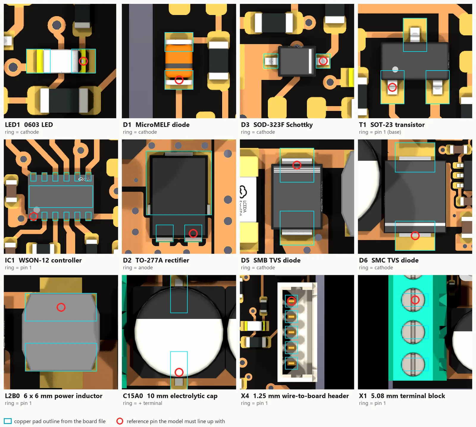
The grid is also easy to share. You can put it in a review, send it to a colleague or hand it to an AI assistant, which can go through the tiles one by one. In our case the assistant flagged the doubtful tiles, and we looked at those closely.
Calibrate first. Our first grid used a pixel scale that was estimated, not measured: 46.5 px/mm instead of the measured 49.2. That 6 % error is invisible near the corner the mapping started from. Across the board it grows to more than 2 mm, so the rings and outlines landed next to the parts and the tiles looked wrong when the models were fine. Before you trust a tile, check that the pad outlines sit on the rendered copper. The figure below shows the effect.
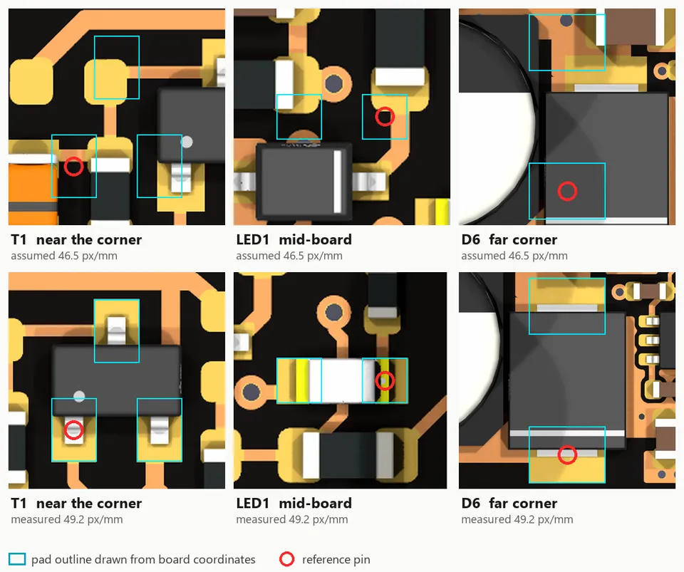
The same method works from below. A bottom-side render (--side bottom, with the x axis mirrored in the mapping) shows through-hole pins in their holes. That is how the 0.48 mm connector offset from Step 3 became obvious.
Results
Every part on the board now has a 3D model except one unmounted option part, for which no model exists online. Ten of the eleven parts that needed models received the manufacturer's exact model from EasyEDA or a matching stock KiCad model. Another 46 passives got their models with the switch to stock footprints. The design rule check reported the same warnings before and after, and the schematic still matched the board.
The checks found real problems that a list of numbers would have hidden:
- a MOSFET rendered 180° off because of the rotation sign
- a connector whose pins missed their holes by about half a millimetre
- eight models that were correct but hidden, because their footprints had no type
- terminal-block holes that were smaller than the manufacturer's footprint
A checklist you can reuse
1. List every footprint with its model and LCSC number.
2. Sort the parts: stock model, exact vendor model, or none available.
3. Download vendor footprints and models with easyeda2kicad --lcsc_id <C-number> --footprint --3d, and keep the files in the project.
4. Find each rotation by comparing your pads with the vendor footprint. Expect the sign to be the opposite of what you calculate.
5. Set the footprint type (SMD or through-hole) so the model isn't hidden.
6. Apply the changes by script to a scratch copy. Run the design rule check, then the real project, with a backup.
7. Render from the top and, for through-hole parts, from below.
8. Measure the pixel scale, then build the grid of tiles with pad outlines and a ring on pin 1.
9. Look at every tile: body inside the outlines, polarity mark at the ring.